カスタムグリッド
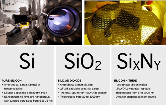
| Si PURE SILICON | SiO SILICON NITRIDE | SiN SILICON OXIDE |
| ●アモルファス, 単結晶, ナノ結晶シリコン ●スパッタ-蒸着 5~50nm膜 ●ナノ結晶フィルムの微細孔 ポアサイズ5~75 nm |
●アモルファス酸化シリコン ●GFLATウルトラフラット膜 ●サーマル, スパッターまたは PECVD蒸着 ●膜厚: 20~4000 nm |
●アモルファス窒化シリコン ●LPCVD低ストレス ●膜厚:5~1000 nm ●ウルトラフラット メンブレン |
カスタムグリッド作製ワークフロー
① 仕様打合せ
② クロムマスクデザイン/プリント
③ Si, SiNまたはSiO 蒸着
④ パタンーニング/エッチング
⑤ 光学, SEM検査
■ SILICON WAFER SPECIFICATIONS
-100, 200, 300 um thick and standard thicknesses
100 & 200um thickness: 100 mm (4-inch) diameter wafer
310um thickness: 150 mm (6-inch) diameter wafer
■ CUSTOM MASK DESIGN AND CHROME MASK PRINTING
-Feature size resolution to 350 nanometers (line/space resolution).
-Minimum membrane window size typically ~5 microns.
-Maximum membrane window size (based on film) up to 25 mm x 25 mm.
■ FRONT-TO-BACK ALIGNMENT LITHOGRAPHY
-Front-to-back tolerance +/-5 microns or better (+/-20 microns for 150mm).
-Features as small as 500 nanometer circles can be etched in suspended membranes.
-Orientation or identification marks can be etched into suspended membrane or over support silicon
to reduce interference with imaging.
■ METAL DEPOSITION
-Deposition of aluminum, palladium, gold, 50 to 200 nm thicknesses
-Deposition of adhesive layer of titanium, chrome, etc.
-Features to less than 10 microns with alignment to membrane windows within +/-5 microns.
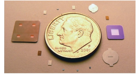
■ DEVICE PACKAGING
-Devices are typically separated from the supporting wafer and packaged in transparent gel-boxes
for ease of handling and viewing.
-All devices are individually inspected under light microscopy.
-Devices can also be designed with continuous films for spin coating that can be later dissected
along scribe lines by the customer.