
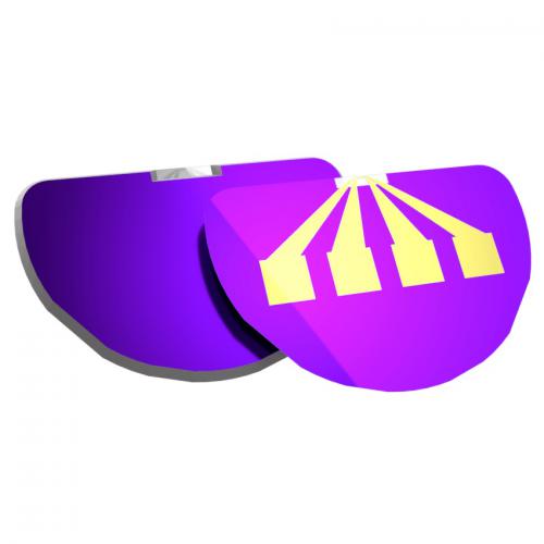
SiN Lift-Out Grids
●Flip-satge FIB/SEMホルダー、TEMホルダーに適合
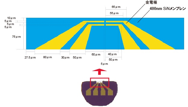
●400nm 膜厚窒化シリコンメンブレン(100 x 500um)
●窒化シリコンメンブレンはFIBにより、電子透過(50nm以下)可能な厚さに加工
●金電極:電気バイアス回路、サンプル加熱アプリケーション
●試料調製、薄膜加工のための簡単にアクセスエッジを提供し、ウィンドウ100 x 500μmの長さに沿って、浮遊側に400nm厚窒化シリコンメンブレンが備えられています
| 型番 | SN100-LFT-AU-2 SN100-LFT-AU |
SN100-LFT |
|---|---|---|
| 品名 | SiN Lift-Out Grid (金電極付) |
SiN Lift-Out Grid |
| イメージ |  |
.jpg) |
| メンブレンサイズ (リフトアウト開口部) |
100 x 500 um | 100 x 500 um |
| メンブレン厚 | SiN 400 nm | SiN 400 nm |
| フレーム厚 | 100 um | 100 um |
| 電極 | 金電極(200nm厚) x 4 | N/A |
| 価格 | SN100-LFT-AU-2 ¥70,000/2枚 |
¥150,000/10枚 |
| SN100-LFT-AU ¥200,000/10枚 |
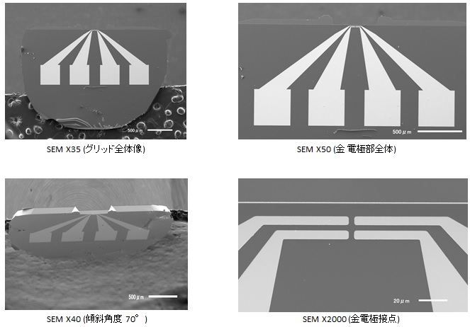
写真提供: 名古屋大学 超高電圧電子顕微鏡施設
Open Half-Grid shape: 自由浮遊側に500 x 100 umの堅牢ウィンドウに400 nm SiNメンブレンを備えており、
試料調整および電子透過のためのFIB薄膜加工が容易に行えます
Gold Contacts: 電気バイアス(電圧/電流)、加熱するための金電極(200 nm厚)がSiNメンブレン上にフォーマットされています
Fit: フレーム厚 100 um厚 Lift-Out gridはSEM/FIB flip stageホルダー、標準TEMホルダーに適合します
アプリケーション: Electrical properties of computer chips, batteries, solar cells, etc
SiNメンブレン/金電極部
APPLICATION NOTE:集束イオンビームによるLift-Out grid試料調整
リフトアウトグリッドは、試料調整を簡素化するために設計されています。このアプリケーションノートでは、従来の
FIB試料調製技術を用いて、リフトアウトグリッドに機械的および電気的に接続する方法を示しています。
.jpg)
Step 1 Load the Lift-Out Grid into the SEM/FIB so the grid edge faces the electron
the sample lamella with a standard u-cut. Next attach the micromanipulator tip to
the top corner of the lamella using a small amount of platinum deposition.
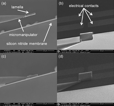
Step 2 Carefully bring the lamella close to the suspended silicon nitride membrane.
Switching back and forth between the SEM imaging mode and the FIB imaging mode
can help give perspective.
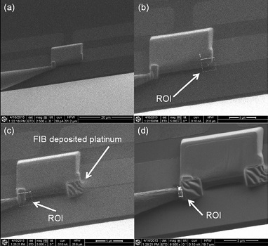
Step 3 Once the lamella is in contact with the membrane, quickly attach a small
amount of FIB deposited platinum to the corner opposite the micromanipulator
connection.
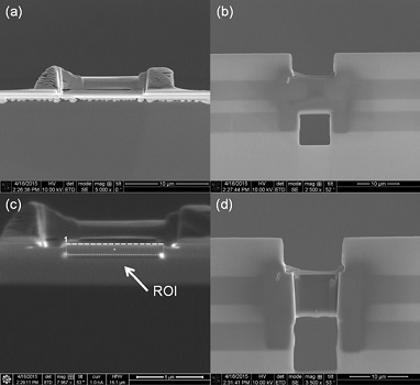
Step 4 Reposition the Lift-Out Grid such that the electron beam is normal to the
silicon nitride membrane. A view through the electron column down onto the
Lift-Out Grid is shown in image (a). In this position the Lift-Out Grid is perpendicular
to its edge-on position relative to the electron beam column used to attach the lamella.
.jpg)
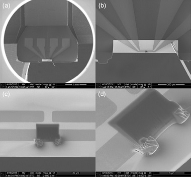
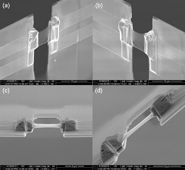
Step 5 With the lamella tacked down and the Lift-Out Grid repositioned, the next
step is to attach the lamella to the metal contacts. Image (a) shows a perspective
view of the lamella before any FIB deposited platinum has been used to attach the
lamella to the contacts.
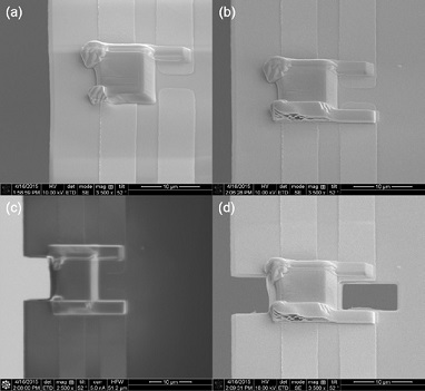
Step 6 Once the FIB deposited platinum connecting the contacts is in place on
one side, it can be placed on the other using the same procedure. Image (a)
shows the lamella before the opposing FIB deposited platinum has been added,
and image (b) shows the lamella after the deposition.
Step 7 After the nitride membrane in front and behind the lamella has been removed,
the lamella is ready to be thinned. (The Lift-Out Grid has been repositioned so that
the lamella is edge-on to the electron beam.)
Step 8 Once the underside of the membrane has been removed, the top and bottom
of the lamella can be thinned using standard lamella thinning techniques. Images (a)
and (b) show the final thinned lamella, with a thickness of ~100-200 nm. Images (c)
and (d) show different perspectives of the Lift-Out Grid and attached lamella. This
particular device is suitable for three different experiments. One is an in situ resistivity
measurement using the four electrical contacts.
Another is a gradient heating experiment: one side is heated, the other left as a cold-sink
and vice versa. Finally, the electrical contacts provide a means of reading out an electron
beam induced current signal from the device.